- despite its relative simplicity, it provides fairly high parameters. Actually, to tell the truth, “chip” amplifiers have a number of limitations, so “loose” amplifiers can provide higher performance. In defense of the microcircuit (otherwise why do I use it myself and recommend it to others?) we can say:
Simple and effective scheme
- the circuit is very simple
- and very cheap
- and requires virtually no adjustment
- and you can assemble it in one evening
- and the quality is superior to many amplifiers of the 70s ... 80s, and is quite sufficient for most applications (and even modern systems under $300 can be inferior to it)
- thus, the amplifier is suitable for both beginners and experienced radio amateurs (for example, I once needed a multi-channel amplifier to test an idea. Guess what I did?).
In any case, a poorly made and incorrectly tuned amplifier in bulk will sound worse than a microcircuit amplifier. And our task is to make a very good amplifier. It should be noted that the sound of the amplifier is very good (if it is made correctly and powered correctly); there is information that some company produced Hi-End amplifiers based on the TDA7294 chip! And our amplifier is no worse!!!
- this is practically a repetition of the connection diagram proposed by the manufacturer. And this is no coincidence - who knows better how to turn it on. And there certainly won’t be any surprises due to non-standard activation or operating mode.
Input path
The input circuit R1C1 is a low pass filter (LPF), cutting off everything above 90 kHz. It is impossible without it - the 21st century is, first of all, the century of high-frequency interference. The cutoff frequency of this filter is quite high. But this is on purpose - I don’t know what this amplifier will be connected to. If there is a volume control at the input, then it will be just right - its resistance will be added to R1, and the cutoff frequency will decrease (the optimal value of the volume control resistance is ~10 kOhm, more is better, but the regulation law will be violated).
Next, the R2C2 chain performs the exact opposite function - it does not allow frequencies below 7 Hz to enter the input. If this is too low for you, the C2 capacity can be reduced. If you get too carried away with reducing capacity, you may be left without any low frequencies at all. For the full audio range, C2 must be at least 0.33 µF. And remember that capacitors have a fairly wide range of capacitances, so if it says 0.47 microfarads, it could easily turn out to be 0.3! And further. At the lower end of the range, the output power is reduced by 2 times, so it is better to choose it lower:
C2[uF] = 1000 / (6.28 * Fmin[Hz] * R2[kOhm])
Resistor R2 sets the input resistance of the amplifier. Its value is slightly larger than according to the datasheet, but this is also better - too low an input impedance may “not be liked” by the signal source. Please note that if a volume control is turned on in front of the amplifier, then its resistance should be 4 times less than R2, otherwise the law of volume control will change (the volume value depends on the angle of rotation of the control). The optimal value of R2 lies in the range of 33...68 kOhm (higher resistance will reduce noise immunity).
Audio amplifier circuit on a chip, namely, the amplifier switching circuit is not inverting. Resistors R3 and R4 create a negative feedback circuit (NFC). The gain is:
Ku = R4 / R3 + 1 = 28.5 times = 29 dB
Gain
This is almost equal to the optimal value of 30 dB. You can change the gain by changing resistor R3. Please note that you cannot make Ku less than 20 - the microcircuit can excite itself. It’s also not worth doing it more than 60 - the depth of feedback will decrease and the distortion will increase. With the resistance values indicated in the diagram, with an input voltage of 0.5 volts, the output power at a 4 ohm load is 50 W. If the sensitivity of the amplifier is not enough, then it is better to use a preamplifier.
The resistance values are slightly higher than those recommended by the manufacturer. Firstly, this increases the input impedance, which is nice for the signal source (to obtain maximum DC balance, R4 must be equal to R2). Secondly, it improves the operating conditions of the electrolytic capacitor C3. And thirdly, it enhances the beneficial effects of C4. More about this. Audio amplifier circuit on a chip works in the following sequence: capacitor C3 in series with R3 creates 100% OOS for direct current (since its resistance to direct current is infinite, and Ku is equal to unity). In order for the influence of C3 on the amplification of low frequencies to be minimal, its capacitance must be quite large. The frequency at which the influence of C3 becomes noticeable is:
f [Hz] = 1000 / (6.28 * R3 [kOhm] * C3 [uF]) = 1.3 Hz
Reducing distortion
This frequency should be very low. The fact is that C3 is electrolytic polar, and it is supplied with alternating voltage and current, which is very bad for it. Therefore, the lower the value of this voltage, the less distortion introduced by C3. For the same purpose, its maximum permissible voltage is chosen to be quite large (50V), although the voltage on it does not exceed 100 millivolts. It is very important that the cutoff frequency of the R3C3 circuit is much lower than the input circuit R2C2. After all, when the influence of C3 manifests itself due to an increase in its resistance, then the voltage on it increases (the output voltage of the amplifier is redistributed between R4, R3 and C3 in proportion to their resistances). If at these frequencies the output voltage drops (due to a drop in the input voltage), then the voltage at C3 does not increase. In principle, you can use a non-polar capacitor as C3, but I can’t say for sure whether this will improve the sound or worse: a non-polar capacitor is “two in one” polar capacitors connected back-to-back.
Capacitor C4 bypasses C3 at high frequencies: electrolytes have another drawback (in fact, there are many drawbacks, this is the price to pay for the high specific capacitance) - they do not work well at frequencies above 5-7 kHz (expensive ones are better, for example Black Gate, which costs 7-7 kHz). 12 euros per piece works well at 20 kHz). Film capacitor C4 “takes over the high frequencies,” thereby reducing the distortion introduced to them by capacitor C3. The larger the C4 capacity, the better. And its maximum operating voltage can be relatively small.
Amplifier stability
Circuit C7R9 increases the stability of the amplifier. In principle, the amplifier is very stable, and you can do without it, but I came across instances of microcircuits that worked worse without this circuit. Capacitor C7 must be designed for a voltage no lower than the supply voltage.
Audio amplifier circuit on a chip, and in particular capacitors C8 and C9 carry out the so-called volt boost. Through them, part of the output voltage flows back into the pre-final stage and is added to the supply voltage. As a result, the supply voltage inside the chip is higher than the voltage of the power supply. This is necessary because the output transistors provide an output voltage 5 volts less than the voltage at their inputs. Thus, in order to get 25 volts at the output, you need to apply a voltage of 30 volts to the gates of the transistors, but where can you get it? So we take it from the exit. Without a voltage boost circuit, the output voltage of the microcircuit would be 10 volts less than the supply voltage, but with this circuit it would be only 2-4. Film capacitor C9 takes over the work at high frequencies, where C8 performs worse. Both capacitors must withstand a voltage not lower than 1.5 times the supply voltage.
Controlling Mute and StdBy modes
Resistors R5-R8, capacitors C5, C6 and diode D1 control the Mute and StdBy modes when the power is turned on and off (see Mute and StandBy modes in the TDA7294/TDA7293 chip). They provide the correct sequence for turning on/off these modes. True, everything works fine even if they are in the “wrong” sequence, so you need such control more for your own pleasure.
Capacitors C10-C13 filter the power. Their use is mandatory - even with the best power supply, the resistance and inductance of the connecting wires can affect the operation of the amplifier. With these capacitors, no wires are a problem (within reasonable limits)! There is no need to reduce the capacity. Minimum 470 µF for electrolytes and 1 µF for film ones. When installing on a board, it is necessary that the leads are as short as possible and well soldered - do not skimp on solder. All these capacitors must withstand a voltage not lower than 1.5 times the supply voltage.
Separation of input and output ground
And finally, resistor R10. It serves to separate the input and output land. “On the fingers” its purpose can be explained as follows. A large current flows from the amplifier output through the load to ground. It may happen that this current, flowing through the “ground” conductor, will also flow through the section through which the input current flows (from the signal source, through the amplifier input, and then back to the source along the “ground”). If the resistance of the conductors was zero, then there would be no problem. But the resistance, although small, is not zero, so a voltage will appear at the resistance of the “ground” wire (Ohm’s law: U=I*R), which will add up to the input. Thus, the output signal of the amplifier will go to the input, and this feedback will not bring anything good, only all sorts of nasty things. The resistance of resistor R10, although small (the optimal value is 1...5 Ohms), is much greater than the resistance of the ground conductor, and through it (the resistor) hundreds of times less current will flow into the input circuit than without it.
In principle, if the board layout is good (and I have a good one), this will not happen, but on the other hand, something similar can happen on a “macro scale” along the signal source-amplifier-load circuit. A resistor will help in this case too. However, it can be completely replaced with a jumper - it was used based on the principle “it’s better to be safe than sorry.”
Power supply
Audio amplifier circuit on a chip is powered by bipolar voltage (i.e. these are two identical sources connected in series, and their common point is connected to ground).
The minimum supply voltage according to the datasheet is +- 10 volts. I personally tried to power it from +-14 volts - the microcircuit works, but is it worth doing this? After all, the output power is scanty! The maximum supply voltage depends on the load resistance (this is the voltage of each arm of the source):
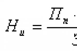
This dependence is caused by the permissible heating of the microcircuit. If the microcircuit is installed on a small radiator, it is better to reduce the supply voltage. The maximum output power received from the amplifier is approximately described by the formula:
where the units are: V, Ohm, W (I will study this issue separately and describe it), and Uip is the voltage of one arm of the power source in silent mode.
Power supply power
The power supply power should be 20 watts more than the output power. The rectifier diodes are designed for a current of at least 10 Amps. The capacitance of the filter capacitors is at least 10,000 µF per arm (less is possible, but the maximum power will decrease and distortion will increase).
It must be remembered that the rectifier voltage at idle is 1.4 times higher than the voltage on the secondary winding of the transformer, so do not burn the microcircuit! A simple but fairly accurate program for calculating a power supply:
PCB layout
Audio amplifier circuit on a chip, the board of which is wired taking into account all the requirements for wiring high-quality amplifiers. The entrance is separated as far as possible from the exit, and is enclosed in a “screen” of divided earth - entrance and exit. The power supply paths ensure maximum efficiency of filter capacitors (at the same time, the length of the leads of capacitors C10 and C12 should be minimal). In my experimental board, I installed terminal blocks for connecting the input, output and power supply - there is a place for them (capacitor C10 may get in the way a little), but for stationary structures it is better to solder all these wires - it’s more reliable.
In addition to low resistance, wide tracks also have the advantage that they are more difficult to peel off when overheated. And when manufacturing using the “laser-ironing” method, if a square of 1 mm x 1 mm is not “printed” anywhere, then it’s not a big deal - the conductor won’t break anyway. In addition, a wide conductor holds heavy parts better (while a thin conductor can simply peel off from the board).
There is only one jumper on the board. It lies under the pins of the microcircuit, so it needs to be mounted first, and leave enough space under the pins so that it doesn’t short out.
All resistors except R9 with a power of 0.12 W, Capacitors C9, C10, C12 K73-17 63V, C4 I used K10-47V 6.8 uF 25V (I had it lying around in the closet... With such a capacitance, even without capacitor C3, the cutoff frequency in the OOS circuit it turns out 20 Hz - where deep bass is not needed, one such capacitor is quite enough). However, I recommend using all capacitors of the K73-17 type. I consider the use of expensive “audiophile” ones to be economically unjustified, and cheap “ceramic” ones will give worse sound (this is in theory, in principle - please just remember that some of them can withstand a voltage of no more than 16 volts and cannot be used as a C7). Any modern electrolytes will do. Audio amplifier circuit on a chip has on the printed circuit board polarity symbols for connecting all electrolytic capacitors and a diode. Diode - any low-power rectifier that can withstand a reverse voltage of at least 50 volts, for example 1N4001-1N4007. It is better not to use high-frequency diodes.
In the corners of the board there is space for holes for M3 mounting screws - you can fasten the board only to the chip body, but it is still more reliable to secure it with screws.
Heat sink for microcircuit
The microcircuit must be installed on a radiator with an area of at least 350 cm2. More is better. In principle, it has thermal protection built into it, but it’s better not to tempt fate. Even if active cooling is assumed, the radiator must still be quite massive: with pulsed heat release, which is typical for music, heat is more effectively removed by the heat capacity of the radiator (i.e., a large cold piece of iron) rather than by dissipation into the environment.
The metal housing of the microcircuit is connected to the negative side of the power supply. This gives rise to two ways to install it on a radiator:
Through an insulating gasket, the radiator can be electrically connected to the housing.
Directly, in this case the radiator is necessarily electrically isolated from the body.
The second option (my favorite) provides better cooling, but requires caution, such as not removing the chip while the power is on.
In both cases, you need to use heat-conducting paste, and in the 1st option it should be applied both between the microcircuit body and the gasket, and between the gasket and the radiator.
Audio amplifier circuit on a microcircuit - setup
Communication on the Internet shows that 90% of all problems with equipment are due to its “not being adjusted.” That is, having soldered yet another circuit and having failed to fix it, the radio amateur gives up on it and publicly declares the circuit bad. Therefore, setup is the most important (and often the most difficult) stage in creating an electronic device.
A properly assembled amplifier does not need adjustment. But, since no one guarantees that all parts are absolutely in good working order, you need to be careful when you turn it on for the first time.
The first switch-on is carried out without load and with the input signal source turned off (it is better to short-circuit the input with a jumper). It would be nice to include fuses of about 1A in the power circuit (both in the plus and minus between the power source and the amplifier itself). Briefly (~0.5 sec.) Apply the supply voltage and make sure that the current consumed from the source is small - the fuses do not burn out. It is convenient if the source has LED indicators - when disconnected from the network, the LEDs continue to light for at least 20 seconds: the filter capacitors are discharged for a long time by the small quiescent current of the microcircuit.
Chip quiescent current
If the current consumed by the microcircuit is large (more than 300 mA), then there can be many reasons: short circuit in installation; poor contact in the “ground” wire from the source; “plus” and “minus” are confused; the pins of the microcircuit touch the jumper; microcircuit is faulty; capacitors C11, C13 are soldered incorrectly; capacitors C10-C13 are faulty.
Making sure that audio amplifier circuit on a chip maintains a normal quiescent current, feel free to turn on the power and measure the constant voltage at the output. Its value should not exceed +-0.05 V. High voltage indicates problems with C3 (less often with C4), or with the microcircuit. There have been cases when the “ground-to-ground” resistor was either poorly soldered or had a resistance of 3 kOhms instead of 3 ohms. At the same time, the output was constant 10...20 volts. By connecting an AC voltmeter to the output, we make sure that the AC voltage at the output is zero (this is best done with the input closed, or simply with the input cable not connected, otherwise there will be noise at the output). The presence of alternating voltage at the output indicates problems with the microcircuit, or circuits C7R9, C3R3R4, R10. Unfortunately, conventional testers often cannot measure the high-frequency voltage that appears during self-excitation (up to 100 kHz), so it is best to use an oscilloscope here.
If everything is in order here, we connect the load, check again for the absence of excitation with the load, and that’s it - you can listen!
Additional testing
But it’s better to do another test. The fact is that the most disgusting type of amplifier excitation, in my opinion, is “ringing” - when excitation appears only in the presence of a signal, and at a certain amplitude. Because it is difficult to detect without an oscilloscope and a sound generator (and it is not easy to eliminate), and the sound deteriorates enormously due to huge inter-modulation distortion. Moreover, this is usually perceived by ear as a “heavy” sound, i.e. without any additional overtones (since the frequency is very high), so the listener does not know that his amplifier is being excited. He just listens and decides that the microcircuit is “bad” and “doesn’t sound.”
If audio amplifier circuit on a microcircuit correctly assembled and a normal power source this should not happen.
However, sometimes it happens, and the C7R9 chain is precisely what struggles with such things. BUT! In a normal microcircuit, everything is OK even in the absence of C7R9. I came across copies of the microcircuit with ringing, in them the problem was solved by introducing the C7R9 circuit (that’s why I use it, even though it’s not in the datasheet). If such a nasty thing occurs even if you have a C7R9, then you can try to eliminate it by “playing” with the resistance (it can be reduced to 3 ohms), but I would not recommend using such a microcircuit - it’s some kind of defect, and who knows? what else will come out in it.
The problem is that the "ringing" can only be seen on an oscilloscope, which is when audio amplifier circuit on a chip receives a signal from a sound generator (you may not notice it on real music) - and not all radio amateurs have this equipment. (Although, if you want to do this business well, try to notice such devices, at least use them somewhere). But if you want high-quality sound, try to check it on the devices - “ringing” is the most insidious thing, and can damage the sound quality in a thousand ways. My boards:

"Desktop" test of the amplifier
Audio amplifier circuit on a chip after preliminary switching on the table, it showed that the circuit and printed circuit board are absolutely working! No additional settings were made after assembly according to the diagram! very satisfied, I recommend!
Preliminary switching on of the amplifier on the table showed that the circuit and printed circuit board are absolutely working! No additional settings were made after assembly according to the diagram! very satisfied, I recommend!
Update- see the bridge version there WK60!!!

What do you think is shown in the photo? So, we don’t give hints from the back rows!
In the meantime, we are looking in a search engine for the inscription on the board, I will tell you what it is. This is the UcD250 module from Hypex Electronics.
Nothing special. Class D, 250 W declared power. Normal, right?
Have the Chinese painted their Watts again? No, today everything is honest and real.
This is the insides of the EveAudio near-field monitor, designed for professional studio work.
The size of the module can be estimated from the photo; for scale, use a regular AA battery.
Digitally controlled preamplifier-switcher. We use programming through the Arduino shell, electronic potentiometers from Microchip, and TFT graphics.

It was not my plan to develop and assemble this device. Well, there’s just no way! I already have two preamps. Both suit me quite well.
But, as usually happens for me, a coincidence of circumstances or a chain of certain events, and now a task has emerged for the near future.
Greetings to Datagor readers again! In the second part we will deal with the construction of a 6-channel volume control.

The regulator consists of two main chips: an ATiny26 microcontroller and a specialized TDA7448 chip. I added a volume indicator (a line of 7 LEDs) to roughly know what level is set, because an infinitely rotating encoder acts as a control knob.

And then I decided to try 5.1 surround sound. But on a budget, without sacrifices. And off we go! I started disassembling, tinkering, designing, assembling, sawing, drilling... In general, I started pumping the system.
I present the results in two parts to dear readers.
By chance, the Arcturus-006-stereo record player fell into my hands. Therefore, there was an urgent need for a phono stage. On the Internet I came across scheme by A. Bokarev, for which I decided to make a much-needed device.
At the back of the player there are two output connectors (SG-5/DIN): one from the built-in phono stage (500mV), the second bypassed for connecting to an external one (5mV). When using the built-in phono stage, a jumper is installed in the second output.
I didn’t like the characteristics of the built-in corrector, and when I turned it on, it turned out that it was faulty - I only heard a 50 Hz hum in the speakers. There was no desire to restore it, so I disconnected the built-in corrector board completely.
I'll listen to my version.

Photo source: vega-brz.ru
The Arctur-006-stereo electric player of the highest complexity group has been produced by the Berdsk Radio Plant since 1983. The player is made on the basis of a two-speed EPU G-2021, with an ultra-low-speed electric motor and direct drive. There is a pressure regulator and a roll force compensator, adjustment of the disc rotation speed using a strobe light, auto-stop, micro-lift, speed switch and auto-return of the tonearm at the end of the record.
This project considers amplifiers for headphones on mass-produced microcircuits, such as BA5415A and BA5417.

I refrained from philosophical discussions about which of the presented sound reproduction schemes is “more correct.” The purpose of the experiments is different - to provide worthy schemes for repetition, and enthusiastic readers will make their own choice and share their impressions.
Currently, a wide range of imported integrated low-frequency amplifiers has become available. Their advantages are satisfactory electrical parameters, the ability to select microcircuits with a given output power and supply voltage, stereophonic or quadraphonic design with the possibility of bridge connection.
To manufacture a structure based on an integral ULF, a minimum of attached parts is required. The use of known-good components ensures high repeatability and, as a rule, no additional tuning is required.
The given typical switching circuits and main parameters of integrated ULFs are designed to facilitate the orientation and selection of the most suitable microcircuit.
For quadraphonic ULFs, the parameters in bridged stereo are not specified.
TDA1010
Supply voltage - 6...24 V
Output power (Un =14.4 V, THD = 10%):
RL=2 Ohm - 6.4 W
RL=4 Ohm - 6.2 W
RL=8 Ohm - 3.4 W
Quiescent current - 31 mA
Connection diagram
TDA1011
Supply voltage - 5.4...20 V
Maximum current consumption - 3 A
Un=16V - 6.5 W
Un=12V - 4.2 W
Un=9V - 2.3 W
Un=6B - 1.0 W
SOI (P=1 W, RL=4 Ohm) - 0.2%
Quiescent current - 14 mA
Connection diagram
TDA1013
Supply voltage - 10...40 V
Output power (THD=10%) - 4.2 W
THD (P=2.5 W, RL=8 Ohm) - 0.15%
Connection diagram
TDA1015
Supply voltage - 3.6...18 V
Output power (RL=4 Ohm, THD=10%):
Un=12V - 4.2 W
Un=9V - 2.3 W
Un=6B - 1.0 W
SOI (P=1 W, RL=4 Ohm) - 0.3%
Quiescent current - 14 mA
Connection diagram
TDA1020
Supply voltage - 6...18 V
RL=2 Ohm - 12 W
RL=4 Ohm - 7 W
RL=8 Ohm - 3.5 W
Quiescent current - 30 mA
Connection diagram
TDA1510
Supply voltage - 6...18 V
Maximum current consumption - 4 A
THD=0.5% - 5.5 W
THD=10% - 7.0 W
Quiescent current - 120 mA
Connection diagram
TDA1514
Supply voltage - ±10...±30 V
Maximum current consumption - 6.4 A
Output power:
Un =±27.5 V, R=8 Ohm - 40 W
Un =±23 V, R=4 Ohm - 48 W
Quiescent current - 56 mA
Connection diagram
TDA1515
Supply voltage - 6...18 V
Maximum current consumption - 4 A
RL=2 Ohm - 9 W
RL=4 Ohm - 5.5 W
RL=2 Ohm - 12 W
RL4 Ohm - 7 W
Quiescent current - 75 mA
Connection diagram
TDA1516
Supply voltage - 6...18 V
Maximum current consumption - 4 A
Output power (Un =14.4 V, THD = 0.5%):
RL=2 Ohm - 7.5 W
RL=4 Ohm - 5 W
Output power (Un =14.4 V, THD = 10%):
RL=2 Ohm - 11 W
RL=4 Ohm - 6 W
Quiescent current - 30 mA
Connection diagram
TDA1517
Supply voltage - 6...18 V
Maximum current consumption - 2.5 A
Output power (Un=14.4B RL=4 Ohm):
THD=0.5% - 5 W
THD=10% - 6 W
Quiescent current - 80 mA
Connection diagram
TDA1518
Supply voltage - 6...18 V
Maximum current consumption - 4 A
Output power (Un =14.4 V, THD = 0.5%):
RL=2 Ohm - 8.5 W
RL=4 Ohm - 5 W
Output power (Un =14.4 V, THD = 10%):
RL=2 Ohm - 11 W
RL=4 Ohm - 6 W
Quiescent current - 30 mA
Connection diagram
TDA1519
Supply voltage - 6...17.5 V
Maximum current consumption - 4 A
Output power (Up=14.4 V, THD=0.5%):
RL=2 Ohm - 6 W
RL=4 Ohm - 5 W
Output power (Un =14.4 V, THD = 10%):
RL=2 Ohm - 11 W
RL=4 Ohm - 8.5 W
Quiescent current - 80 mA
Connection diagram
TDA1551
Supply voltage -6...18 V
THD=0.5% - 5 W
THD=10% - 6 W
Quiescent current - 160 mA
Connection diagram
TDA1521
Supply voltage - ±7.5...±21 V
Output power (Un=±12 V, RL=8 Ohm):
THD=0.5% - 6 W
THD=10% - 8 W
Quiescent current - 70 mA
Connection diagram
TDA1552
Supply voltage - 6...18 V
Maximum current consumption - 4 A
Output power (Un =14.4 V, RL = 4 Ohm):
THD=0.5% - 17 W
THD=10% - 22 W
Quiescent current - 160 mA
Connection diagram
TDA1553
Supply voltage - 6...18 V
Maximum current consumption - 4 A
Output power (Up=4.4 V, RL=4 Ohm):
THD=0.5% - 17 W
THD=10% - 22 W
Quiescent current - 160 mA
Connection diagram
TDA1554
Supply voltage - 6...18 V
Maximum current consumption - 4 A
THD=0.5% - 5 W
THD=10% - 6 W
Quiescent current - 160 mA
Connection diagram
TDA2004
Output power (Un=14.4 V, THD=10%):
RL=4 Ohm - 6.5 W
RL=3.2 Ohm - 8.0 W
RL=2 Ohm - 10 W
RL=1.6 Ohm - 11 W
KHI (Un=14.4V, P=4.0 W, RL=4 Ohm) - 0.2%;
Bandwidth (at -3 dB level) - 35...15000 Hz
Quiescent current -<120 мА
Connection diagram
TDA2005
Dual integrated ULF, designed specifically for use in cars and allowing operation with low-impedance loads (up to 1.6 Ohms).
Supply voltage - 8...18 V
Maximum current consumption - 3.5 A
Output power (Up = 14.4 V, THD = 10%):
RL=4 Ohm - 20 W
RL=3.2 Ohm - 22 W
SOI (Uп =14.4 V, Р=15 W, RL=4 Ohm) - 10%
Bandwidth (level -3 dB) - 40...20000 Hz
Quiescent current -<160 мА
Connection diagram
TDA2006
The pin layout matches the pin layout of the TDA2030 chip.
Supply voltage - ±6.0...±15 V
Maximum current consumption - 3 A
Output power (Ep=±12V, THD=10%):
at RL=4 Ohm - 12 W
at RL=8 Ohm - 6...8 W THD (Ep=±12V):
at P=8 W, RL= 4 Ohm - 0.2%
at P=4 W, RL= 8 Ohm - 0.1%
Bandwidth (at -3 dB level) - 20...100000 Hz
Consumption current:
at P=12 W, RL=4 Ohm - 850 mA
at P=8 W, RL=8 Ohm - 500 mA
Connection diagram
TDA2007
Dual integrated ULF with single-row pin arrangement, specially designed for use in television and portable radio receivers.
Supply voltage - +6...+26 V
Quiescent current (Ep=+18 V) - 50...90 mA
Output power (THD=0.5%):
at Ep=+18 V, RL=4 Ohm - 6 W
at Ep=+22 V, RL=8 Ohm - 8 W
SOI:
at Ep=+18 V P=3 W, RL=4 Ohm - 0.1%
at Ep=+22 V, P=3 W, RL=8 Ohm - 0.05%
Bandwidth (at -3 dB level) - 40...80000 Hz
Connection diagram
TDA2008
Integrated ULF, designed to operate on low-impedance loads, providing high output current, very low harmonic content and intermodulation distortion.
Supply voltage - +10...+28 V
Quiescent current (Ep=+18 V) - 65...115 mA
Output power (Ep=+18V, THD=10%):
at RL=4 Ohm - 10...12 W
at RL=8 Ohm - 8 W
SOI (Ep= +18 V):
at P=6 W, RL=4 Ohm - 1%
at P=4 W, RL=8 Ohm - 1%
Maximum current consumption - 3 A
Connection diagram
TDA2009
Dual integrated ULF, designed for use in high-quality music centers.
Supply voltage - +8...+28 V
Quiescent current (Ep=+18 V) - 60...120 mA
Output power (Ep=+24 V, THD=1%):
at RL=4 Ohm - 12.5 W
at RL=8 Ohm - 7 W
Output power (Ep=+18 V, THD=1%):
at RL=4 Ohm - 7 W
at RL=8 Ohm - 4 W
SOI:
at Ep= +24 V, P=7 W, RL=4 Ohm - 0.2%
at Ep= +24 V, P=3.5 W, RL=8 Ohm - 0.1%
at Ep= +18 V, P=5 W, RL=4 Ohm - 0.2%
at Ep= +18 V, P=2.5 W, RL=8 Ohm - 0.1%
Maximum current consumption - 3.5 A
Connection diagram
TDA2030
Integrated ULF, providing high output current, low harmonic content and intermodulation distortion.
Supply voltage - ±6...±18 V
Quiescent current (Ep=±14 V) - 40...60 mA
Output power (Ep=±14 V, THD = 0.5%):
at RL=4 Ohm - 12...14 W
at RL=8 Ohm - 8...9 W
SOI (Ep=±12V):
at P=12 W, RL=4 Ohm - 0.5%
at P=8 W, RL=8 Ohm - 0.5%
Bandwidth (at -3 dB level) - 10...140000 Hz
Consumption current:
at P=14 W, RL=4 Ohm - 900 mA
at P=8 W, RL=8 Ohm - 500 mA
Connection diagram
TDA2040
Integrated ULF, providing high output current, low harmonic content and intermodulation distortion.
Supply voltage - ±2.5...±20 V
Quiescent current (Ep=±4.5...±14 V) - mA 30...100 mA
Output power (Ep=±16 V, THD = 0.5%):
at RL=4 Ohm - 20...22 W
at RL=8 Ohm - 12 W
THD (Ep=±12V, P=10 W, RL = 4 Ohm) - 0.08%
Maximum current consumption - 4 A
Connection diagram
TDA2050
Integrated ULF, providing high output power, low harmonic content and intermodulation distortion. Designed to work in Hi-Fi stereo systems and high-end TVs.
Supply voltage - ±4.5...±25 V
Quiescent current (Ep=±4.5...±25 V) - 30...90 mA
Output power (Ep=±18, RL = 4 Ohm, THD = 0.5%) - 24...28 W
SOI (Ep=±18V, P=24Wt, RL=4 Ohm) - 0.03...0.5%
Bandwidth (at -3 dB level) - 20...80000 Hz
Maximum current consumption - 5 A
Connection diagram
TDA2051
Integrated ULF, which has a small number of external elements and provides low harmonic content and intermodulation distortion. The output stage operates in class AB, which allows for greater output power.
Output power:
at Ep=±18 V, RL=4 Ohm, THD=10% - 40 W
at Ep=±22 V, RL=8 Ohm, THD=10% - 33 W
Connection diagram
TDA2052
Integrated ULF, the output stage of which operates in class AB. Accepts a wide range of supply voltages and has a high output current. Designed for use in television and radio receivers.
Supply voltage - ±6...±25 V
Quiescent current (En = ±22 V) - 70 mA
Output power (Ep = ±22 V, THD = 10%):
at RL=8 Ohm - 22 W
at RL=4 Ohm - 40 W
Output power (En = 22 V, THD = 1%):
at RL=8 Ohm - 17 W
at RL=4 Ohm - 32 W
SOI (with a passband at the level of -3 dB 100... 15000 Hz and Pout = 0.1... 20 W):
at RL=4 Ohm -<0,7 %
at RL=8 Ohm -<0,5 %
Connection diagram
TDA2611
Integrated ULF designed for use in household equipment.
Supply voltage - 6...35 V
Quiescent current (Ep=18 V) - 25 mA
Maximum current consumption - 1.5 A
Output power (THD=10%): at Ep=18 V, RL=8 Ohm - 4 W
at Ep=12V, RL=8 0m - 1.7 W
at Ep=8.3 V, RL=8 Ohm - 0.65 W
at Ep=20 V, RL=8 Ohm - 6 W
at Ep=25 V, RL=15 Ohm - 5 W
THD (at Pout=2 W) - 1%
Bandwidth - >15 kHz
Connection diagram
TDA2613
SOI:
(Ep=24 V, RL=8 Ohm, Pout=6 W) - 0.5%
(En=24 V, RL=8 Ohm, Pout=8 W) - 10%
Quiescent current (Ep=24 V) - 35 mA
Connection diagram
TDA2614
Integrated ULF, designed for use in household equipment (television and radio receivers).
Supply voltage - 15...42 V
Maximum current consumption - 2.2 A
Quiescent current (Ep=24 V) - 35 mA
SOI:
(Ep=24 V, RL=8 Ohm, Pout=6.5 W) - 0.5%
(Ep=24 V, RL=8 Ohm, Pout=8.5 W) - 10%
Bandwidth (level -3 dB) - 30...20000 Hz
Connection diagram
TDA2615
Dual ULF, designed for use in stereo radios or televisions.
Supply voltage - ±7.5...21 V
Maximum current consumption - 2.2 A
Quiescent current (Ep=7.5...21 V) - 18...70 mA
Output power (Ep=±12 V, RL=8 Ohm):
THD=0.5% - 6 W
THD=10% - 8 W
Bandwidth (at level -3 dB and Pout = 4 W) - 20...20000 Hz
Connection diagram
TDA2822
Dual ULF, designed for use in portable radios and television receivers.
Quiescent current (Ep=6 V) - 12 mA
Output power (THD=10%, RL=4 Ohm):
Ep=9V - 1.7 W
Ep=6V - 0.65 W
Ep=4.5V - 0.32 W
Connection diagram
TDA7052
ULF designed for use in battery-powered wearable audio devices.
Supply voltage - 3...15V
Maximum current consumption - 1.5A
Quiescent current (E p = 6 V) -<8мА
Output power (Ep = 6 V, R L = 8 Ohm, THD = 10%) - 1.2 W
Connection diagram
TDA7053
Dual ULF, designed for use in wearable audio devices, but can also be used in any other equipment.
Supply voltage - 6...18 V
Maximum current consumption - 1.5 A
Quiescent current (E p = 6 V, R L = 8 Ohm) -<16 mA
Output power (E p = 6 V, RL = 8 Ohm, THD = 10%) - 1.2 W
SOI (E p = 9 V, R L = 8 Ohm, Pout = 0.1 W) - 0.2%
Operating frequency range - 20...20000 Hz
Connection diagram
TDA2824
Dual ULF designed for use in portable radio and television receivers
Supply voltage - 3...15 V
Maximum current consumption - 1.5 A
Quiescent current (Ep=6 V) - 12 mA
Output power (THD=10%, RL=4 Ohm)
Ep=9 V - 1.7 W
Ep=6 V - 0.65 W
Ep=4.5 V - 0.32 W
THD (Ep=9 V, RL=8 Ohm, Pout=0.5 W) - 0.2%
Connection diagram
TDA7231
ULF with a wide range of supply voltages, designed for use in portable radios, cassette recorders, etc.
Supply voltage - 1.8...16 V
Quiescent current (Ep=6 V) - 9 mA
Output power (THD=10%):
En=12B, RL=6 Ohm - 1.8 W
En=9B, RL=4 Ohm - 1.6 W
Ep=6 V, RL=8 Ohm - 0.4 W
Ep=6 V, RL=4 Ohm - 0.7 W
Ep=3 V, RL=4 Ohm - 0.11 W
Ep=3 V, RL=8 Ohm - 0.07 W
THD (Ep=6 V, RL=8 Ohm, Pout=0.2 W) - 0.3%
Connection diagram
TDA7235
ULF with a wide range of supply voltages, designed for use in portable radio and television receivers, cassette recorders, etc.
Supply voltage - 1.8...24 V
Maximum current consumption - 1.0 A
Quiescent current (Ep=12 V) - 10 mA
Output power (THD=10%):
Ep=9 V, RL=4 Ohm - 1.6 W
Ep=12 V, RL=8 Ohm - 1.8 W
Ep=15 V, RL=16 Ohm - 1.8 W
Ep=20 V, RL=32 Ohm - 1.6 W
THD (Ep=12V, RL=8 Ohm, Pout=0.5 W) - 1.0%
Connection diagram
TDA7240
Quiescent current (Ep=14.4 V) - 120 mA
RL=4 Ohm - 20 W
RL=8 Ohm - 12 W
SOI:
(Ep=14.4 V, RL=8 Ohm, Pout=12W) - 0.05%
Connection diagram
TDA7241
Bridged ULF, designed for use in car radios. It has protection against short circuits in the load, as well as overheating.
Maximum supply voltage - 18 V
Maximum current consumption - 4.5 A
Quiescent current (Ep=14.4 V) - 80 mA
Output power (Ep=14.4 V, THD=10%):
RL=2 Ohm - 26 W
RL=4 Ohm - 20 W
RL=8 Ohm - 12 W
SOI:
(Ep=14.4 V, RL=4 Ohm, Pout=12 W) - 0.1%
(Ep=14.4 V, RL=8 Ohm, Pout=6 W) - 0.05%
Bandwidth level -3 dB (RL=4 Ohm, Pout=15 W) - 30...25000 Hz
Connection diagram
TDA1555Q
Supply voltage - 6...18 V
Maximum current consumption - 4 A
Output power (Up = 14.4 V. RL = 4 Ohm):
- THD=0.5% - 5 W
- THD=10% - 6 W Quiescent current - 160 mA
Connection diagram
TDA1557Q
Supply voltage - 6...18 V
Maximum current consumption - 4 A
Output power (Up = 14.4 V, RL = 4 Ohm):
- THD=0.5% - 17 W
- THD=10% - 22 W
Quiescent current, mA 80
Connection diagram
TDA1556Q
Supply voltage -6...18 V
Maximum current consumption -4 A
Output power: (Up=14.4 V, RL=4 Ohm):
- THD=0.5%, - 17 W
- THD=10% - 22 W
Quiescent current - 160 mA
Connection diagram
TDA1558Q
Supply voltage - 6..18 V
Maximum current consumption - 4 A
Output power (Up=14 V, RL=4 Ohm):
- THD=0.6% - 5 W
- THD=10% - 6 W
Quiescent current - 80 mA
Connection diagram
TDA1561
Supply voltage - 6...18 V
Maximum current consumption - 4 A
Output power (Up=14V, RL=4 Ohm):
- THD=0.5% - 18 W
- THD=10% - 23 W
Quiescent current - 150 mA
Connection diagram
TDA1904
Supply voltage - 4...20 V
Maximum current consumption - 2 A
Output power (RL=4 Ohm, THD=10%):
- Up=14 V - 4 W
- Up=12V - 3.1 W
- Up=9 V - 1.8 W
- Up=6 V - 0.7 W
SOI (Up=9 V, P<1,2 Вт, RL=4 Ом) - 0,3 %
Quiescent current - 8...18 mA
Connection diagram
TDA1905
Supply voltage - 4...30 V
Maximum current consumption - 2.5 A
Output power (THD=10%)
- Up=24 V (RL=16 Ohm) - 5.3 W
- Up=18V (RL=8 Ohm) - 5.5 W
- Up=14 V (RL=4 Ohm) - 5.5 W
- Up=9 V (RL=4 Ohm) - 2.5 W
SOI (Up=14 V, P<3,0 Вт, RL=4 Ом) - 0,1 %
Quiescent current -<35 мА
Connection diagram
TDA1910
Supply voltage - 8...30 V
Maximum current consumption - 3 A
Output power (THD=10%):
- Up=24 V (RL=8 Ohm) - 10 W
- Up=24 V (RL=4 Ohm) - 17.5 W
- Up=18 V (RL=4 Ohm) - 9.5 W
SOI (Up=24 V, P<10,0 Вт, RL=4 Ом) - 0,2 %
Quiescent current -<35 мА
Connection diagram
TDA2003
Supply voltage - 8...18 V
Maximum current consumption - 3.5 A
Output power (Up=14V, THD=10%):
- RL=4.0 Ohm - 6 W
- RL=3.2 Ohm - 7.5 W
- RL=2.0 Ohm - 10 W
- RL=1.6 Ohm - 12 W
SOI (Up=14.4 V, P<4,5 Вт, RL=4 Ом) - 0,15 %
Quiescent current -<50 мА
Connection diagram
TDA7056
ULF designed for use in portable radio and television receivers.
Supply voltage - 4.5...16 V Maximum current consumption - 1.5 A
Quiescent current (E p = 12 V, R = 16 Ohm) -<16 мА
Output power (E P = 12 V, R L = 16 Ohm, THD = 10%) - 3.4 W
THD (E P = 12 V, R L = 16 Ohm, Pout = 0.5 W) - 1%
Operating frequency range - 20...20000 Hz
Connection diagram
TDA7245
ULF designed for use in wearable audio devices, but can also be used in any other equipment.Supply voltage - 12...30 V
Maximum current consumption - 3.0 A
Quiescent current (E p = 28 V) -<35 мА
Output power (THD = 1%):
-E p = 14 V, R L = 4 Ohm - 4 W
-E P = 18 V, R L = 8 Ohm - 4 W
Output power (THD = 10%):
-E P = 14 V, R L = 4 Ohm - 5 W
-E P = 18 V, R L = 8 Ohm - 5 W
SOI,%
-E P = 14 V, R L = 4 Ohm, Pout<3,0 - 0,5 Вт
-E P = 18 V, R L = 8 Ohm, Pout<3,5 - 0,5 Вт
-E P = 22 V, RL = 16 Ohm, Pout<3,0 - 0.4 Вт
Bandwidth by level
-ZdB(E =14 V, PL = 4 Ohm, Pout = 1 W) - 50...40000 Hz
TEA0675
Two-channel Dolby B noise suppressor designed for automotive applications. Contains pre-amplifiers, an electronically controlled equalizer, and an electronic pause detection device for the Automatic Music Search (AMS) scanning mode. Structurally, it is carried out in SDIP24 and SO24 housings.Supply voltage, 7.6,..12 V
Current consumption, 26...31 mA
Ratio (signal+noise)/signal, 78...84 dB
Harmonic distortion factor:
at a frequency of 1 kHz, 0.08...0.15%
at a frequency of 10 kHz, 0.15...0.3%
Output impedance, 10 kOhm
Voltage gain, 29...31 dB
TEA0678
Two-channel integrated Dolby B noise suppressor designed for use in car audio equipment. Includes pre-amplifier stages, electronically controlled equalizer, electronic signal source switcher, Automatic Music Search (AMS) system.Available in SDIP32 and SO32 packages.
Current consumption, 28 mA
Preamp gain (at 1 kHz), 31 dB
Harmonic distortion
< 0,15 %
at a frequency of 1 kHz at Uout=6 dB,< 0,3 %
Noise voltage, normalized to the input, in the frequency range 20...20000 Hz at Rist=0, 1.4 µV
TEA0679
Two-channel integrated amplifier with Dolby B noise reduction system, designed for use in various car audio equipment. Includes pre-amplification stages, an electronically controlled equalizer, an electronic signal source switch, and an Automatic Music Search (AMS) system. The main IC adjustments are controlled via the I2C busAvailable in SO32 housing.
Supply voltage, 7.6...12 V
Current consumption, 40 mA
Harmonic distortion
at a frequency of 1 kHz at Uout=0 dB,< 0,15 %
at a frequency of 1 kHz at Uout=10 dB,< 0,3 %
Crosstalk attenuation between channels (Uout=10 dB, at a frequency of 1 kHz), 63 dB
Signal+noise/noise ratio, 84 dB
TDA0677
Dual pre-amplifier-equalizer designed for use in car radios. Includes a preamplifier and a corrector amplifier with an electronic time constant switch. Also contains an electronic input switch.The IC is manufactured in the SOT137A package.
Supply voltage, 7.6.,.12 V
Current consumption, 23...26 mA
Signal+noise/noise ratio, 68...74 dB
Harmonic distortion:
at a frequency of 1 kHz at Uout = 0 dB, 0.04...0.1%
at a frequency of 10 kHz at Uout = 6 dB, 0.08...0.15%
Output impedance, 80... 100 Ohm
Gain:
at a frequency of 400 Hz, 104...110 dB
at a frequency of 10 kHz, 80..86 dB
TEA6360
Two-channel five-band equalizer, controlled via 12C bus, designed for use in car radios, televisions, and music centers.Manufactured in SOT232 and SOT238 packages.
Supply voltage, 7... 13.2 V
Current consumption, 24.5 mA
Input voltage, 2.1 V
Output voltage, 1 V
Reproducible frequency range at level -1dB, 0...20000 Hz
Nonlinear distortion coefficient in the frequency range 20...12500 Hz and output voltage 1.1 V, 0.2...0.5%
Transfer coefficient, 0.5...0 dB
Operating temperature range, -40...+80 C
TDA1074A
Designed for use in stereo amplifiers as a two-channel tone control (low and mid frequencies) and sound. The chip includes two pairs of electronic potentiometers with eight inputs and four separate output amplifiers. Each potentiometric pair is adjusted individually by applying constant voltage to the corresponding terminals.The IC is manufactured in SOT102, SOT102-1 packages.
Maximum supply voltage, 23 V
Current consumption (no load), 14...30 mA
Gain, 0 dB
Harmonic distortion:
at a frequency of 1 kHz at Uout = 30 mV, 0.002%
at a frequency of 1 kHz at Uout = 5 V, 0.015...1%
Output noise voltage in the frequency range 20...20000 Hz, 75 µV
Interchannel isolation in the frequency range 20...20000 Hz, 80 dB
Maximum power dissipation, 800 mW
Operating temperature range, -30...+80°С
TEA5710
A functionally complete IC that performs the functions of an AM and FM receiver. Contains all the necessary stages: from a high-frequency amplifier to an AM/FM detector and a low-frequency amplifier. It is characterized by high sensitivity and low current consumption. Used in portable AM/FM receivers, radio timers, radio headphones. The IC is manufactured in the SOT234AG (SOT137A) package.Supply voltage, 2..,12 V
Consumption current:
in AM mode, 5.6...9.9 mA
in FM mode, 7.3...11.2 mA
Sensitivity:
in AM mode, 1.6 mV/m
in FM mode at signal-to-noise ratio 26 dB, 2.0 µV
Harmonic distortion:
in AM mode, 0.8..2.0%
in FM mode, 0.3...0.8%
Low frequency output voltage, 36...70 mV
I'd say it's just a super simple amp that contains all four elements and puts out 40 watts of power into two channels!
4 parts and 40 W x 2 power output Karl! This is a godsend for car enthusiasts, since the amplifier is powered by 12 Volts, the full range is from 8 to 18 Volts. It can be easily integrated into subwoofers or speaker systems.
Everything is accessible today thanks to the use of modern element base. Namely the chip - TDA8560Q.
This is a PHILIPS chip. Previously, the TDA1557Q was in use, on which you can also build a stereo amplifier with an output power of 22 W. But it was later modernized by updating the output stage and the TDA8560Q appeared with an output power of 40 W per channel. Also similar is the TDA8563Q.
Car amplifier circuit on a chip
The diagram shows a microcircuit, two input capacitors and one filter capacitor. The filter capacitor is specified with a minimum capacity of 2200 uF, but the best solution would be to take 4 of these capacitors and parallel them, this will ensure more stable operation of the amplifier at low frequencies. The microcircuit must be installed on a radiator, the larger the better.Building a simple amplifier


It is also possible to increase the number of components in the circuit that increase reliability during operation, but not fundamentally.

Five more details have been added here, I’ll explain why. Two 10K Ohm resistors will remove the hum if there are long wires going to the circuit. A 27 K Ohm resistor and a 47 uF capacitor provide a smooth start of the amplifier without clicks. A 220 pF capacitor will filter out high-frequency noise traveling along the power wires. So I recommend modifying the circuit with these nodes; it won’t be superfluous.
I would also like to add that the amplifier develops full power only at a 2 Ohm load. At 4 Ohms there will be somewhere around 25 W, which is also very good. So our Soviet acoustics will be rocked.
Low-voltage, single-polar power supply provides additional advantages: it can be used in car speakers, but at home it can be powered from an old computer power supply.
The minimum number of components allows you to build in an amplifier to replace an old one that has failed on a microcircuit of other brands.
Ganichev G.
Moscow
This article continues a series of publications devoted to power amplifiers offered to radio amateurs by MASTER KIT. The article includes two recent developments - NM2042 (powerful low-frequency amplifier 140 W) and NM2043 (powerful automotive bridge Hi-Fi low-frequency amplifier 4x77 W). The amplifiers are designed taking into account all the necessary requirements and are made on a modern integrated element base. The offered PAs have high performance characteristics, high reliability, ease of manufacture/connection and an optimal price/quality ratio, which is an important factor today. You can assemble the devices from the MASTER KIT kits NM2042 and NM2043.
MASTER KIT specialists were given, and successfully solved, the task of preparing technical documentation and producing a line of ULFs for use in Hi-Fi audio equipment. Gradually, the range of these devices is expanded and supplemented with new developments. This article will discuss two new developments - and.
All proposed models of power amplifiers have a minimum level of self-noise, a minimum level of nonlinear distortion and a wide reproducible frequency band. Models differ mainly in maximum output power, supply voltage (bipolar or unipolar “automotive” (14.4 V)), number of amplification channels and external design.
Radio amateurs can wire a printed circuit board themselves, but it must be taken into account that this is a very responsible and serious job. Not everyone knows that, for example, incorrect routing of printed conductors in a powerful amplifier can increase the level of its nonlinear distortion tenfold or even render it inoperable altogether. Therefore, professional designers specializing in this field were involved in the development of printed circuit boards.
. Powerful low frequency amplifier 140 W (TDA7293).
The proposed low-frequency amplifier has a minimum nonlinear distortion coefficient and noise level. The device has small dimensions. A wide range of supply voltages and load resistances expands the scope of application of this PA. It can be used both outdoors for various events and at home as part of your musical audio complex. The amplifier has proven itself well as a ULF for a subwoofer.
The ULF is made on the TDA7293 integrated circuit. This IC is a class AB ULF. Thanks to a wide range of supply voltages and the ability to deliver current to a load of up to 10 A, the microcircuit provides the same maximum output power at loads from 4 Ohms to 8 Ohms. One of the main features of this microcircuit is the use of field-effect transistors in the preliminary and output amplification stages and the ability to parallel connect several ICs to operate with low-impedance loads (< 4 Ом).
The operating mode of the IC is controlled using switch SW1. To turn on the ULF, SW1 must be closed. Switch SW2 is provided for technological purposes. For normal operation, SW2 must be jumpered in position 2-3.
Coil L1 must be made independently. L1 – frameless, three-layer, contains ten turns of PEV-1.0 wire in each layer. Winding must be carried out on a 12 mm mandrel. Approximate inductance – 5 µH.
The supply voltage is supplied to contacts X3 (+), X6 (-) and X7 (common).
The signal source is connected to X1(+) and X2(common).
The load is connected to X4(+) and X5(common).
Structurally, the amplifier is made on a printed circuit board made of foil fiberglass. The design provides for installation of the board into the case; for this purpose, mounting holes are provided along the edges of the board for 2.5 mm screws. For the convenience of connecting the supply voltage, signal source and load, the board has reserved spaces for terminal screw clamps.
Structurally, a dual logical input of control signals MUTE/ST-BY is provided for “soft” activation of the ULF.
The amplifier chip must be installed on a heat sink (not included in the kit) with an area of at least 600 cm2. As a radiator, you can use the metal case or chassis of the device into which the ULF is installed. During installation, it is recommended to use heat-conducting paste type KTP-8 to increase the reliability of the IC.
The general view of the amplifier is shown in Fig. 1, the electrical circuit diagram in Fig. 2, the arrangement of elements on the board and the connection of the amplifier in Fig. 3, the view of the printed circuit board from the side of the conductors in Fig. 4. The list of elements is given in Table 2.
Table 1. Technical characteristics.
| Supply voltage, bipolar, V | +/- 12...50 |
| Peak output current, A | 10 |
| Current in quiescent mode, mA | 30 |
| Current in MUTE/ST-BY mode, mA | 0,5 |
| Output power, W at harmonic distortion = 1%, Up = +/- 30 V, Rн = 4 Ohm | 80 |
| Output power, W at harmonic distortion = 10%, Up = +/- 45 V, Rн = 8 Ohm | 140 |
| Output power, W at harmonic distortion = 10%, Up = +/- 30 V, Rн = 4 Ohm | 110 |
| Gain Au, dB | 30 |
| Reproducible frequency range, Hz | 20...20000 |
| Input impedance, kOhm | 22 |
| PCB dimensions, mm | 47x55 |
Table 2. List of elements.
| Position | Name | Col. |
| C1 | 470 pF | |
| C2 | 0.47 µF | |
| C3, C10 | 22 µF/63 V | |
| C4, C5 | 10 µF/63 V | |
| C6, C7, C11 | 0.1 µF | |
| C8, C9 | 1000 µF/63 V | |
| DA1 | TDA7293 | |
| L1 | 5 µH | |
| R1 | 1 kOhm | |
| R2 | 10 kOhm | |
| R3 | 30 kOhm | |
| R4, R5, R9...R12 | 22 kOhm | |
| R6 | 20 kOhm | |
| R7 | 680 Ohm | |
| R8, R14 | 4.7 ohm | |
| R13 | 270 Ohm | |
| VD1 | 1N4148 |
Fig1. General view of the NM2042 amplifier.

Fig.2. Electrical circuit diagram of the NM2042 amplifier.

Fig.3. Layout of elements on the board and connection of the NM2042 amplifier.

Fig.4. View of the printed circuit board from the side of the printed conductors of the NM2042 amplifier.
. Powerful car bridge Hi-Fi low frequency amplifier 4X77 W (TDA7560).
The main purpose of this ULF is to install it in your car radio, instead of an old low-frequency amplifier, to increase its output power or for outdoor events using a 12 V battery as the main power source for the equipment. Thanks to the use of a bridge circuit, the amplifier develops power up to 80 W into a 2 Ohm load in each of the four channels. A special feature of the amplifier is the use of field-effect transistors in the output stages. The device has small dimensions, a wide range of supply voltages and load resistances.
The ULF is made on an integrated circuit TDA7560 (DA1). This IC is a class AB ULF and is installed in car audio devices to obtain a high-quality, powerful output music signal. The IC is designed to operate with a load of 4...2 Ohms, signal distortion meets Hi-Fi requirements. The microcircuit has protection against short-circuit load and overheating. Features of the microcircuit include the use of field-effect transistors in the output stages. The microcircuit contains four identical bridge amplifiers with a power of up to 80 W into a 2 Ohm load.
Switches SW1 (ST-BY) and SW2 (MUTE) are designed to control the operating modes of the IC. Closing the contacts in SW1 controls the ST-BY (standby/working) mode, and SW2 controls the MUTE (pause) mode.
Particular attention should be paid to connecting the microcircuit to the power source:
The IC is extremely sensitive to supply voltage - a maximum of 18 V.
Reversing the polarity of the supply voltage source leads to failure of the IC (Urev = 6 V maximum).
The supply voltage is connected to contacts X9(+) and X10(-).
Signal sources are connected to X1(+),X2(-);X3(+),X4(-);X5(+),X6(-);X7(+),X8(-).
The amplified signal is removed from contacts X11, X12; X13, X14; X15, X16; X17, X18.
The general view of the amplifier is shown in Fig. 5, the electrical circuit diagram in Fig. 6, the arrangement of elements on the board and the connection of the amplifier in Fig. 7, the top view of the printed circuit board in Fig. 8, the bottom view of the printed circuit board in Fig. 9. The list of elements is given in Table 3.
Table 3. Technical characteristics.
Table 4. List of elements