Very often, in the process of technical creativity, it is necessary to manufacture printed circuit boards for mounting electronic circuits. And now I will talk about one of the most, in my opinion, advanced methods for manufacturing printed circuit boards using a laser printer and an iron. We live in the 21st century, so we will make our work easier by using a computer.
Step 1. Board design
Design printed circuit board we will be in a specialized program. For example, in the program sprint Layout 4.

Step 2. Printing the board pattern
After that, we need to print the board drawing. To do this, we will do the following:
- In the printer settings, turn off all the toner saving options, and if there is an appropriate regulator, set the maximum saturation.
- Let's take an A4 sheet from some unnecessary magazine. The paper should be coated and preferably a minimum of drawing on it.
- We will print the printed circuit board pattern on coated paper in a mirror image. It is better to have several copies at once.

Step 3Cleaning the Board
Let's put the printed sheet aside for now and start preparing the board. Foiled getinaks, foiled textolite can serve as the starting material for the board. During long-term storage, copper foil becomes covered with a film of oxides, which can interfere with etching. So let's start preparing the board. petty sandpaper peel off the oxide film from the board. Don't be too zealous, the foil is thin. Ideally, the board after stripping should shine.

Step 4 Degreasing the Board
After stripping, rinse the board with running water. After that, you need to degrease the board in order for the toner to stick better. You can degrease with any household detergent, or by washing with an organic solvent (for example, gasoline or acetone)

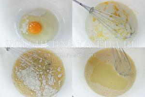
Step 5. Transferring the drawing to the board
After that, using an iron, we transfer the drawing from the sheet to the board. We put the printout with a pattern on the board and start ironing with a hot iron, evenly heating the entire board. The toner will start to melt and stick to the board. The time and effort of warming up is selected experimentally. It is necessary that the toner does not spread, but it is also necessary that it is all welded.

Step 6. Cleaning the board from paper
After the board with the piece of paper stuck to it cools down, we wet it and roll it with our fingers under a stream of water. Wet paper will clump, and adhered toner will remain in place. The toner is quite durable and is difficult to scrape off with a fingernail.

Step 7 Etching the Board
Etching of printed circuit boards is best done in ferric chloride (III) Fe Cl 3. This reagent is sold at any radio parts store and is inexpensive. Immerse the board in the solution and wait. The etching process depends on the freshness of the solution, its concentration, etc. It can take from 10 minutes to an hour or more. The process can be accelerated by shaking the bath with the solution.

The end of the process is determined visually - when all unprotected copper is etched.

The toner is washed off with acetone.

Step 8: Drill holes
Drilling is usually carried out with a small motor with a collet chuck (all this is in the radio parts store). Drill diameter for conventional elements 0.8 mm. If necessary, holes are drilled with a large diameter drill.
Tahiti! .. Tahiti! ..
We have not been to any Tahiti!
We are well fed here!
© Cartoon cat
Introduction with digression
How were boards made before in domestic and laboratory conditions? There were several ways, for example:
- drew future conductors with penguins;
- engraved and cut with cutters;
- they glued adhesive tape or electrical tape, then the drawing was cut out with a scalpel;
- the simplest stencils were made, followed by drawing with an airbrush.
The missing elements were drawn with drawing pen and retouched with a scalpel.
It was a long and laborious process, requiring remarkable artistic abilities and accuracy from the “drawer”. The thickness of the lines hardly fit into 0.8 mm, there was no repetition accuracy, each board had to be drawn separately, which greatly hindered the release of even a very small batch printed circuit boards(further PP).
What do we have today?
Progress does not stand still. The times when radio amateurs painted PP with stone axes on mammoth skins have sunk into oblivion. The appearance on the market of publicly available chemistry for photolithography opens up completely different prospects for the production of PP without metallizing holes at home.
Let's take a quick look at the chemistry used to make PP today.
Photoresist
You can use liquid or film. Film in this article will not be considered due to its scarcity, the difficulties of rolling to the PCB and the lower quality of the printed circuit boards obtained at the output.
After analyzing the market offers, I settled on POSITIV 20 as the optimal photoresist for home production PP.
Purpose:
POSITIV 20 photosensitive varnish. It is used in small-scale production of printed circuit boards, engravings on copper, when carrying out work related to the transfer of images to various materials.
Properties:
High exposure characteristics ensure good contrast of transferred images.
Application:
It is used in areas related to the transfer of images to glass, plastics, metals, etc. in small-scale production. The method of application is indicated on the bottle.
Characteristics:
Color: blue
Density: at 20°C 0.87 g/cm3
Drying time: at 70°C 15 min.
Consumption: 15 l/m2
Maximum photosensitivity: 310-440nm
The instructions for the photoresist say that you can store it at room temperature and it is not subject to aging. Strongly disagree! It should be stored in a cool place, for example, on the bottom shelf of the refrigerator, where the temperature is usually maintained at +2+6°C. But in no case do not allow negative temperatures!
If you use photoresists that are sold "in bulk" and do not have light-tight packaging, you need to take care of protection from light. It is necessary to store in total darkness and temperature +2+6°C.
Enlightener
Similarly, I find TRANSPARENT 21, which I use all the time, to be the most suitable illuminator.
Purpose:
Allows direct transfer of images to surfaces coated with POSITIV 20 photosensitive emulsion or other photoresist.
Properties:
Gives transparency to paper. Provides UV light transmission.
Application:
For quick transfer of contours of drawings and diagrams to the substrate. Allows you to significantly simplify the process of reproduction and reduce time s e costs.
Characteristics:
Color: transparent
Density: at 20°C 0.79 g/cm3
Drying time: at 20°C 30 min.
Note:
Instead of plain paper with an illuminator, you can use a transparent film for inkjet or laser printers depending on what we will print the photomask on.
Photoresist Developer
There are many different solutions for developing photoresist.
It is advised to manifest with a solution " liquid glass". His chemical composition: Na 2 SiO 3 *5H 2 O. This substance has a huge number of advantages. The most important thing is that it is very difficult to overexpose the BP in it you can leave the BP for a non-fixed time. The solution almost does not change its properties with temperature changes (there is no risk of decomposition with increasing temperature), it also has a very long term storage its concentration remains constant for at least a couple of years. The absence of the problem of overexposure in the solution will make it possible to increase its concentration in order to reduce the time of manifestation of PP. It is recommended to mix 1 part concentrate with 180 parts water (a little over 1.7 g of silicate in 200 ml of water), but it is possible to make a more concentrated mixture so that the image develops in about 5 seconds without the risk of surface damage due to overexposure. If it is not possible to purchase sodium silicate, use sodium carbonate (Na 2 CO 3) or potassium carbonate (K 2 CO 3).
I have not tried either the first or the second, so I will tell you what I have been showing without any problems for several years now. I use an aqueous solution of caustic soda. For 1 liter cold water 7 grams of caustic soda. If there is no NaOH, I use a KOH solution, doubling the concentration of alkali in the solution. Development time 30-60 seconds with correct exposure. If, after 2 minutes, the pattern does not appear (or appears weakly), and the photoresist begins to wash off from the workpiece, it means that the exposure time has not been chosen correctly: you need to increase it. If, on the contrary, it quickly appears, but both the illuminated areas and the unexposed areas are washed off - either the concentration of the solution is too high, or the quality of the photomask is poor (ultraviolet passes freely through the “black”): you need to increase the print density of the template.
Copper pickling solutions
Excess copper from printed circuit boards is etched using various etchants. Among people doing this at home, ammonium persulfate, hydrogen peroxide + hydrochloric acid, copper sulfate solution + table salt are often common.
I always poison with ferric chloride in glassware. When working with the solution, you need to be careful and attentive: if it gets on clothes and objects, rusty spots remain, which are difficult to remove with a weak solution of citric (lemon juice) or oxalic acid.
We heat the concentrated solution of ferric chloride to 50-60 ° C, immerse the workpiece in it, gently and effortlessly drive the glass rod with a cotton swab at the end through areas where copper is worse etched, this achieves more even etching over the entire area of the PCB. If the speed is not forced to equalize, the required duration of etching increases, and this eventually leads to the fact that in areas where copper has already been etched, etching of the tracks begins. As a result, we do not have what we wanted to get. It is highly desirable to ensure continuous mixing pickling solution.
Chemistry for removing photoresist
What is the easiest way to wash off the already unnecessary photoresist after etching? After repeated trial and error, I settled on ordinary acetone. When it is not there, I wash it off with any solvent for nitro paints.
So, we make a printed circuit board
Where does a high quality PCB start? Right:
Creating a high quality photomask
For its manufacture, you can use almost any modern laser or inkjet printer. Given that we are using a positive photoresist in this article, where copper should remain on the PCB, the printer should draw black. Where there should be no copper the printer should not draw anything. Very important point when printing a photomask: it is required to set the maximum ink watering (in the settings of the printer driver). The more black the shaded areas are, the more likely you are to get a great result. Color is not needed, a black cartridge is enough. From that program (we will not consider programs: everyone is free to choose for himself from PCAD to Paintbrush), in which the photomask was drawn, we print on a regular sheet of paper. The higher the resolution when printing and the better the paper, the higher the quality of the photomask will be. I recommend at least 600 dpi, the paper should not be very thick. When printing, we take into account that the side of the sheet on which the paint is applied, the template will be placed on the PP blank. If done otherwise, the edges of the PCB conductors will be blurry, fuzzy. Let the paint dry if it was an inkjet printer. Next, we impregnate TRANSPARENT 21 paper, let it dry and the photomask is ready.
Instead of paper and an illuminator, it is possible and even very desirable to use a transparent film for laser (when printing on a laser printer) or inkjet (for inkjet printing) printers. Please note that these films have unequal sides: only one working. If you use laser printing, I highly recommend doing a "dry" run of a sheet of film before printing just run the sheet through the printer, simulating printing, but not printing anything. Why is this needed? When printing, the fuser (oven) will heat up the sheet, which will inevitably lead to its deformation. As a consequence, there is an error in the PP geometry at the output. In the manufacture of double-sided PP, this is fraught with a mismatch of layers with all the consequences And with the help of a “dry” run, we will warm up the sheet, it will deform and will be ready for printing a template. When printing, the sheet will pass through the oven a second time, but the deformation will be much less significant checked repeatedly.
If the PCB is simple, you can draw it manually in a very convenient program with a Russified interface Sprint Layout 3.0R (~650 KB).

On preparatory stage draw not too bulky electrical circuits very convenient in the also Russified program sPlan 4.0 (~450 KB).

This is how ready-made photomasks printed on an Epson Stylus Color 740 printer look like:


We print only in black, with the maximum watering of the dye. Material transparent film for inkjet printers.
Preparing the PCB surface for photoresist application
For the production of PP are used sheet materials coated with copper foil. The most common options are with a copper thickness of 18 and 35 microns. Most often, for the production of PP at home, sheet textolite (a fabric pressed with glue in several layers), fiberglass (the same thing, but epoxy compounds are used as glue) and getinaks (pressed paper with glue) are used. Less often sittal and polycor (high-frequency ceramics are rarely used at home), fluoroplast (organic plastic). The latter is also used for the manufacture of high-frequency devices and, having very good electrical characteristics, can be used anywhere and everywhere, but its high price limits its use.
First of all, you need to make sure that the workpiece does not have deep scratches, burrs and corroded areas. Next, it is desirable to polish the copper to a mirror. We polish without being particularly zealous, otherwise we will erase the already thin layer of copper (35 microns) or, in any case, we will achieve different thicknesses of copper on the surface of the workpiece. And this, in turn, will lead to different speed Etching: Erases faster where it is thinner. And a thinner conductor on the board is not always good. Especially if it is long and a decent current will flow through it. If the copper on the workpiece is of high quality, without sins, then it is enough to degrease the surface.
Deposition of photoresist on the surface of the workpiece
We place the board on a horizontal or slightly inclined surface and apply the composition from an aerosol package from a distance of about 20 cm. Remember that the most important enemy in this case is dust. Every particle of dust on the surface of the workpiece is a source of problems. To create a uniform coating, spray the spray in a continuous zigzag motion, starting from the top left corner. Do not overspray as this causes unwanted streaks and results in uneven coating thickness requiring longer exposure times. Summer high temperature environment re-treatment may be required, or aerosol may need to be sprayed from a shorter distance to reduce evaporative loss. When spraying, do not tilt the can strongly this leads to an increased consumption of propellant gas and, as a result, aerosol can stops working, although there is still photoresist in it. If you get unsatisfactory results with spray coating of photoresist, use spin coating. In this case, the photoresist is applied to a board mounted on a rotating table with a drive of 300-1000 rpm. After finishing the coating, the board should not be exposed to strong light. By the color of the coating, you can approximately determine the thickness of the applied layer:
- light gray blue 1-3 microns;
- dark gray blue 3-6 microns;
- blue 6-8 microns;
- dark blue over 8 microns.
On copper, the color of the coating may have a greenish tinge.
The thinner the coating on the workpiece, the better the result.
I always apply photoresist on a centrifuge. In my centrifuge, the rotation speed is 500-600 rpm. Fastening should be simple, clamping is done only at the ends of the workpiece. We fix the workpiece, start the centrifuge, spray on the center of the workpiece and observe how the photoresist spreads over the surface in a thin layer. By centrifugal forces, excess photoresist will be thrown off the future PCB, so I highly recommend providing a protective wall so as not to turn workplace in a pigsty. I use an ordinary pan, in the bottom of which a hole is made in the center. The axis of the electric motor passes through this hole, on which a mounting platform in the form of a cross of two aluminum rails is installed, along which the ears of the workpiece clamp “run”. The ears are made of aluminum corners clamped on the rail with a wing nut. Why aluminum? Small specific gravity and, as a result, less runout when the center of mass of rotation deviates from the center of rotation of the centrifuge axis. The more precisely the workpiece is centered, the less beating will be due to the eccentricity of the mass and the less effort will be required to rigidly fasten the centrifuge to the base.
Photoresist applied. Let it dry for 15-20 minutes, turn the workpiece over, apply a layer on the second side. We give another 15-20 minutes to dry. Do not forget that direct sunlight and fingers on the working sides of the workpiece are unacceptable.
Tanning of photoresist on the workpiece surface
We place the workpiece in the oven, gradually bring the temperature to 60-70 ° C. At this temperature we maintain 20-40 minutes. It is important that nothing touches the surfaces of the workpiece only touching the ends is allowed.
Alignment of the upper and lower photomasks on the surfaces of the workpiece
On each of the photomasks (upper and lower) there should be marks, according to which 2 holes must be made on the workpiece to match the layers. The farther apart the marks, the higher the alignment accuracy. I usually place them diagonally across the templates. According to these marks on the workpiece, using a drilling machine, we drill two holes strictly at 90 ° (the thinner the holes, the more accurate the alignment - I use a 0.3 mm drill) and combine the templates along them, not forgetting that the template must be applied to the photoresist the side that was printed on. We press the templates to the workpiece with thin glasses. It is preferable to use quartz glasses they transmit ultraviolet better. Plexiglas (plexiglass) gives even better results, but it has an unpleasant scratching property, which will inevitably affect the quality of the PP. At small sizes PP can use the transparent cover from the packaging of the CD. In the absence of such glasses, ordinary window glass can also be used, increasing the exposure time. It is important that the glass is even, ensuring that the photomasks fit evenly on the workpiece, otherwise it will not be possible to obtain high-quality track edges on the finished PCB.

A blank with a photomask under plexiglass. We use the box from under the CD.
Exposure (flare)
The time required for exposure depends on the thickness of the photoresist layer and the intensity of the light source. POSITIV 20 photoresist varnish is sensitive to ultraviolet rays, the maximum sensitivity falls on the area with a wavelength of 360-410 nm.
It is best to expose under lamps whose radiation range is in the ultraviolet region of the spectrum, but if you do not have such a lamp, ordinary powerful incandescent lamps can be used, increasing the exposure time. Do not start illumination until the illumination from the source stabilizes it is necessary that the lamp warms up for 2-3 minutes. The exposure time depends on the thickness of the coating and is usually 60-120 seconds when the light source is located at a distance of 25-30 cm. The glass plates used can absorb up to 65% of ultraviolet, so in such cases it is necessary to increase the exposure time. top scores achieved using transparent plexiglass plates. When using a photoresist with long term storage exposure time may need to be doubled remember: photoresists are subject to aging!
Examples of using different light sources:


UV lamps
We expose each side in turn, after the exposure we let the blank stand for 20-30 minutes in a dark place.
Development of the exposed workpiece
Develop in NaOH solution ( caustic soda) see the beginning of the article for details at a solution temperature of 20-25°C. If there is no manifestation up to 2 minutes small O exposure time. If it appears well, but useful areas are also washed off you are too smart with the solution (the concentration is too high) or the exposure time is too long with this radiation source or the photomask is of poor quality insufficiently saturated printed black color allows ultraviolet light to illuminate the workpiece.
When developing, I always very carefully, effortlessly “roll” a cotton swab on a glass rod in those places where the exposed photoresist should be washed off, this speeds up the process.
Washing the workpiece from alkali and residues of exfoliated exposed photoresist
I do this under a faucet—normal tap water.
Retanning photoresist
We place the workpiece in the oven, gradually raise the temperature and at a temperature of 60-100 ° C we hold for 60-120 minutes the pattern becomes strong and solid.
Checking the development quality
For a short time (for 5-15 seconds) we immerse the workpiece in a solution of ferric chloride heated to a temperature of 50-60 ° C. Rinse quickly with running water. In places where there is no photoresist, intensive etching of copper begins. If a photoresist is accidentally left somewhere, carefully mechanically remove it. It is convenient to do this with a conventional or ophthalmic scalpel, armed with optics (soldering glasses, loupes A watchmaker, loop A on a tripod, microscope).
Etching
We pickle in a concentrated solution of ferric chloride with a temperature of 50-60°C. It is desirable to ensure continuous circulation of the pickling solution. We gently “massage” badly etched places with a cotton swab on a glass rod. If the ferric chloride is freshly prepared, the pickling time usually does not exceed 5-6 minutes. We wash the workpiece with running water.


Board etched
How to prepare a concentrated solution of ferric chloride? We dissolve FeCl 3 in slightly (up to 40 ° C) heated water until it ceases to dissolve. Filter the solution. Store in a dark, cool place in an airtight, non-metallic package in glass bottles, For example.
Removing unwanted photoresist
We wash off the photoresist from the tracks with acetone or a solvent for nitro-paints and nitro-enamels.
Hole drilling
It is advisable to select the diameter of the point of the future hole on the photomask in such a way that it would be convenient to drill later. For example, with the required hole diameter of 0.6-0.8 mm, the dot diameter on the photomask should be about 0.4-0.5 mm in this case, the drill will center well.
It is advisable to use tungsten carbide-coated drills: HSS drills wear out very quickly, although steel can be used for drilling single holes large diameter(greater than 2 mm), as tungsten carbide coated drills of this diameter are too expensive. When drilling holes with a diameter of less than 1 mm, it is better to use vertical machine otherwise your drill bits will break quickly. If drilling hand drill Distortions are inevitable, leading to inaccurate joining of holes between layers. Movement from top to bottom on a vertical drilling machine the most optimal in terms of the load on the tool. Carbide drills are made with a rigid (i.e. the drill exactly fits the diameter of the hole) or with a thick (sometimes called "turbo") shank having standard size(usually 3.5 mm). When drilling with carbide-coated drills, it is important to firmly fix the PCB, since such a drill, when moving up, can lift the PCB, skew the perpendicularity and tear out a piece of the board.
Drills with small diameters are usually inserted into either collet(various sizes), or in a three-jaw chuck. For precise locking, clamping in a three-jaw chuck is not the most the best option, and a small drill size (less than 1 mm) quickly grooves in the jaws, losing good hold. Therefore, for drill diameter less than 1 mm, it is better to use a collet chuck. Just in case, get an extra set containing spare collets for each size. Some inexpensive drills are made with plastic collets - throw them away and buy metal ones.
To obtain acceptable accuracy, it is necessary to properly organize the workplace, that is, firstly, to ensure good lighting of the board when drilling. To do this, you can use a halogen lamp, attaching it to a tripod to be able to choose a position (illuminate the right side). Secondly, raise the work surface about 15 cm above the countertop for better visual control over the process. It would be nice to remove dust and chips during the drilling process (you can use a regular vacuum cleaner), but this is not necessary. It should be noted that the dust from fiberglass generated during drilling is very caustic and irritates the skin if it comes into contact with it. And finally, when working, it is very convenient to use the foot switch of the drilling machine.
Typical hole sizes:
- vias 0.8 mm or less;
- integrated circuits, resistors, etc. 0.7-0.8 mm;
- large diodes (1N4001) 1.0 mm;
- contact blocks, trimmers up to 1.5 mm.
Try to avoid holes with a diameter of less than 0.7 mm. Always keep at least two spare drills 0.8 mm or less, as they always break just at the moment when you urgently need to order. Drills 1mm and larger are much more reliable, although it would be nice to have spare ones for them. When you need to make two identical boards, you can drill them at the same time to save time. In this case, it is necessary to very carefully drill holes in the center of the pad near each corner of the PCB, and for large boards, holes located close to the center. Lay the boards on top of each other and, using the 0.3mm centering holes in two opposite corners and the pins as pegs, secure the boards against each other.
If necessary, you can countersink holes with drills of a larger diameter.
Copper tinning on PP
If you need to irradiate the tracks on the PCB, you can use a soldering iron, soft low-melting solder, alcohol-rosin flux and coaxial cable braid. With large volumes, they are tinned in bathtubs filled with low-temperature solders with the addition of fluxes.
The most popular and simple melt for tinning is the low-melting alloy "Rose" (tin 25%, lead 25%, bismuth 50%), the melting point of which is 93-96 ° C. The board is placed with tongs under the level of the liquid melt for 5-10 seconds and, having taken it out, it is checked whether the entire copper surface is covered evenly. If necessary, the operation is repeated. Immediately after removing the board from the melt, its residues are removed either with a rubber squeegee or by sharp shaking in a direction perpendicular to the plane of the board, while holding it in the clamp. Another way to remove residues of the Rose alloy is to heat the board in an oven and shake it. The operation can be repeated to achieve a mono-thick coating. To prevent oxidation of the hot melt, glycerin is added to the tinning tank so that its level covers the melt by 10 mm. After the end of the process, the board is washed from glycerin in running water. Attention! These operations involve working with installations and materials that are under the influence of high temperature, therefore, to prevent burns, it is necessary to use protective gloves, goggles and aprons.
The tin-lead tinning operation proceeds similarly, but more heat melt limits the scope of this method in terms of handicraft production.
Do not forget to clean the board from flux after tinning and degrease thoroughly.
If you have a large production you can use chemical tinning.
Applying a protective mask
The operations with applying a protective mask exactly repeat everything that was written above: we apply a photoresist, dry, tan, center the photomasks of the masks, expose, develop, wash and tan again. Of course, we skip the steps with checking the quality of development, etching, removing photoresist, tinning and drilling. At the very end, we tan the mask for 2 hours at a temperature of about 90-100 ° C it will become strong and hard, like glass. The formed mask protects the surface of the PCB from external influences and protects against theoretically possible short circuits during operation. It also plays an important role in automatic soldering does not allow the solder to “sit down” on neighboring areas, closing them.
That's it, the double-sided printed circuit board with the mask is ready.
I had to make PP in this way with the width of the tracks and the step between them up to 0.05 mm (!). But this is a piece of jewelry. And without much effort, you can make PP with a track width and a step between them of 0.15-0.2 mm.
On the board shown in the photographs, I did not apply a mask there was no such need.


Printed circuit board in the process of mounting components on it
And here is the device itself, for which the software was made:

This is a cellular telephone bridge that allows you to reduce the cost of mobile services by 2-10 times for this it was worth messing around with PP;). The PCB with soldered components is in the stand. Previously, there was an ordinary charger for mobile phone batteries.
Additional Information
Hole plating
At home, you can even metallize holes. For this inner surface holes are treated with a 20-30% solution of silver nitrate (lapis). Then the surface is cleaned with a squeegee and the board is dried in the light (you can use a UV lamp). The essence of this operation is that under the action of light, silver nitrate decomposes, and inclusions of silver remain on the board. Next, copper is chemically precipitated from the solution: copper sulfate (copper sulfate) 2 g, sodium hydroxide 4 g, ammonia 25% 1 ml, glycerin 3.5 ml, formalin 10% 8-15 ml, water 100 ml. The shelf life of the prepared solution is very short it is necessary to prepare immediately before use. After the copper is deposited, the board is washed and dried. The layer is obtained very thin, its thickness must be increased to 50 microns by galvanizing.
Electroplating solution for copper plating:
For 1 liter of water, 250 g of copper sulfate (copper sulfate) and 50-80 g of concentrated sulfuric acid. The anode is a copper plate suspended parallel to the part to be coated. The voltage should be 3-4 V, current density 0.02-0.3 A / cm 2, temperature 18-30 ° C. The lower the current, the slower the metallization process, but the better the resulting coating.

Fragment of the printed circuit board, where the metallization is visible in the hole
Homemade photoresists
Photoresist based on gelatin and potassium bichromate:
First solution: pour 15 g of gelatin into 60 ml of boiled water and leave to swell for 2-3 hours. After swelling of the gelatin, place the container in a water bath at a temperature of 30-40 ° C until the gelatin is completely dissolved.
The second solution: in 40 ml of boiled water, dissolve 5 g of potassium dichromate (chromic peak, bright orange powder). Dissolve in low ambient light.
Pour the second into the first solution with vigorous stirring. Add a few drops of ammonia to the resulting mixture with a pipette until a straw color is obtained. The photographic emulsion is applied to the prepared board in very low light. The board dries to "tack" at room temperature in complete darkness. After exposure, wash the board in low diffused light in warm running water until the untanned gelatin is removed. To better evaluate the result, you can stain areas with unremoved gelatin with a solution of potassium permanganate.
Advanced Homemade Photoresist:
First solution: 17 g of wood glue, 3 ml of an aqueous solution of ammonia, 100 ml of water, leave to swell for a day, then heat in a water bath at 80 ° C until completely dissolved.
Second solution: 2.5 g potassium dichromate, 2.5 g ammonium dichromate, 3 ml aqueous ammonia solution, 30 ml water, 6 ml alcohol.
When the first solution has cooled to 50°C, pour the second solution into it with vigorous stirring and filter the resulting mixture ( this and subsequent operations must be carried out in a darkened room, sunlight unacceptable!). The emulsion is applied at a temperature of 30-40°C. Further as in the first recipe.
Photoresist based on ammonium dichromate and polyvinyl alcohol:
We prepare a solution: polyvinyl alcohol 70-120 g / l, ammonium dichromate 8-10 g / l, ethyl alcohol 100-120 g / l. Avoid bright light! Apply in 2 coats: first coat drying 20-30 minutes at 30-45°C second coat drying 60 minutes at 35-45°C. Developer 40% ethanol solution.
Chemical tinning
First of all, the board must be decapitated in order to remove the formed copper oxide: 2-3 seconds in a 5% hydrochloric acid solution, followed by rinsing in running water.
It is enough to simply carry out chemical tinning by immersing the board in an aqueous solution containing tin chloride. The release of tin on the surface of the copper coating occurs when immersed in a solution of tin salt, in which the copper potential is more electronegative than the coating material. A change in the potential in the desired direction is facilitated by the introduction of a complexing additive thiocarbamide (thiourea) into the tin salt solution. Solutions of this type have the following composition (g/l):
Among the listed solutions, solutions 1 and 2 are the most common. Sometimes it is proposed to use as a surfactant for the 1st solution. detergent"Progress" in the amount of 1 ml / l. The addition of 2-3 g/l of bismuth nitrate to the 2nd solution leads to the precipitation of an alloy containing up to 1.5% bismuth, which improves the solderability of the coating (prevents aging) and greatly increases the shelf life before soldering the components of the finished PP.
To preserve the surface, aerosol sprays based on fluxing compositions are used. After drying, the varnish applied to the surface of the workpiece forms a strong, smooth film that prevents oxidation. One of the popular substances is "SOLDERLAC" from Cramolin. Subsequent soldering is carried out directly on the treated surface without additional varnish removal. In especially critical cases of soldering, the varnish can be removed with an alcohol solution.
Artificial tinning solutions deteriorate over time, especially when exposed to air. Therefore, if you do not often have large orders, then try to prepare at once a small amount of solution, sufficient to tin the required amount of PP, and store the remaining solution in a closed container (bottles of the type used in the photograph are ideal, which do not let air through). It is also necessary to protect the solution from contamination, which can greatly degrade the quality of the substance.
In conclusion, I want to say that it is still better to use ready-made photoresists and not bother with plating holes at home - you still won’t get great results.
Many thanks to the candidate of chemical sciences Filatov Igor Evgenievich for advice on chemistry-related matters.
I also want to express my gratitude Igor Chudakov.
» Electronics printed circuit board - manufacturing instructions
The practice of design and installation, directly related to electronics, cannot do without the main part - the printed circuit board. The initial development of some electronic device is, of course, permissible with the help of surface mounting. However, a full-fledged printed circuit board will still have to be made if we are talking about a serious electronic device. There are two options: order the manufacture of a printed circuit board in a service or make a printed circuit board with your own hands directly at home. The first option requires a solid financial investment and two to three weeks of waiting. The second requires nothing but personal desire, a piece of foil textolite and a small amount of ferric chloride.
 It is quite possible to obtain such a result of work at home using simple available funds, tools, materials
If you master all the intricacies of production and stock up necessary material, the manufacture of printed circuit boards at home is not excluded, if not on an industrial scale, then in quantities sufficient for business.
There are several technologies for drawing and etching miniature tracks on foil textolite. Starting from the method of a simple drawing of an electronic circuit with nail polish, followed by chemical etching, and ending with automatic laser wiring and micron cutting.
However, for home conditions, a special technique is required - effective, but at the same time budgetary and relatively uncomplicated.
PCB manufacturing at home
Here - as part of a kind of tutorial, is considered using the technology of transferring toner with a laser printer.
This method has been developed for a long time, but is still accompanied by a lot of new tips and tricks, thanks to which the efficiency only increases.
What does a home electronics engineer need?
- design program,
- laser printer,
- any glossy magazine,
- household iron,
- one or two plastic containers,
- small brush or toothbrush
- latex gloves,
- ferric chloride,
- foil textolite.
Almost all components of the list can be found in the household. The exceptions are: ferric chloride and textolite with foil.
 Two materials: iron chloride and foil textolite, which you will need to buy. Everything else is usually available among household items and materials.
 These two list items are closed through a visit to an electronics store or radio market. Such outlets are available in any medium-sized settlement. IN last resort, you can order both components online.
Meanwhile, ferric chloride is quite replaceable by another chemical, obtained on the basis of a mixture of copper sulphate (MC) and common table salt (PS). The mixture is made in the ratio of 1 part of MK to 2 parts of PS, diluted in 0.5 liters of boiling water.
Usually, for the manufacture of a medium-sized electronic printed circuit board, it is enough to take 4 tablespoons of MK and 2 tablespoons of PS. Thoroughly stir the powder mixture poured with boiling water and let it stand.
The only difference between such a solution and FeCl 3 is a slightly longer etching time. But on the other hand, a mixture on copper sulphate is safer than FeCl 3. Copper sulfate (powdered) is available at any hardware store.
Creating a PCB design
To create a PCB pattern design, the KiCad computer program seems to be optimal - a professional tool for drawing electronic printed circuit boards, but at the same time free.
The KiCad software provides the user with a brush routing function, making it easy to route differential pairs, interactively adjust the length of the trace.
 The working window of the KiCad program, a professional layout tool that is indispensable in the PCB manufacturing process. The software is distributed free of charge
  Toner print on glossy magazine page. As you can see from the figure, the print quality is quite high. The same mark should be on the printed circuit board foil.
 The factor of the presence of third-party images does not have any effect on the process. In any case, the printer toner drawing remains on the glossy surface of the magazine page (paper). And this is exactly the result that you want to get.
It is advisable to print twice (on two different pages) to make sure that the printed pattern does not have spots, smears, or other defects.
Transferring wiring from printer to foil
If the trace of the printed circuit board layout is qualitatively issued by a laser printer, the glossy page of the magazine with the resulting print should be carefully removed from the printer and placed pattern-side down on the copper surface of the textolite.
 Heat treatment of a printed circuit board using a conventional household iron. Heating temperature - maximum. Otherwise, the quality of the transfer suffers.
 The heated sole of the iron presses a magazine sheet with a printed layout of the circuit to the surface of the foil textolite. Hold the iron on the sheet without moving for about 30 seconds.
Next, you need to smooth the surface of the sheet with an iron in circular motions for 2-3 minutes. During this period of time, by thermal treatment, the toner firmly adheres to the copper coating of the textolite.
 The result of transferring a toner print from a magazine page to the copper coating of the textolite. Looks no worse than the industrial version
 The completion of the process of transferring the imprint onto the textolite copper foil is the removal of the glued magazine sheet. This requires patience and accuracy.
Consider the process of manufacturing printed circuit boards at home on specific example. You need to make two boards. One is an adapter from one type of housing to another. The second is the replacement of a large microcircuit with a BGA package with two smaller ones, with TO-252 packages, with three resistors. Board sizes: 10x10 and 15x15 mm. There are several options for making printed circuit boards at home. The most popular - with the help of photoresist and "iron-laser technology".
Instructions for making printed circuit boards at home
You will need
- personal computer with a program for tracing printed circuit boards;
- laser printer;
- thick paper;
- fiberglass;
- iron;
- hacksaw;
- acid for etching the board.
1 Project preparation printed circuit board
Preparing a PCB project. I use the DipTrace program: convenient, fast, high quality. Developed by our compatriots. Very convenient and pleasant user interface, in contrast to the generally recognized PCAD. Free for small projects. Libraries of cases of radio-electronic components, including 3D models. There is a conversion to PCAD PCB format. Many domestic firms have already begun to accept projects in the DipTrace format.
PCB project
The DipTrace program has the ability to see the future creation in volume, which is convenient and visual. This is what I should get (the boards are shown at different scales):

2 markup fiberglass
First, we mark the textolite and cut out the blank for printed circuit boards.

3 Project Output on a laser printer
We output the project on a laser printer in a mirror image in the highest possible quality, without skimping on toner. Through long experiments, the best paper for this was chosen - thick matte paper for printers. You can try using photo paper or buy special thermal paper.

4 Transferring a project on fiberglass
Clean and degrease the board blank. If there is no degreaser, you can walk on the copper foil of fiberglass with an ordinary eraser. Next, using an iron, we “weld” the toner from the paper to the future printed circuit board. I hold for 3-4 minutes under slight pressure, until the paper turns slightly yellow. I set the heat to max. I put another sheet of paper on top for more even heating, otherwise the image may “float”.
An important point here is the uniformity of heating and pressure and the heating time. If the iron is underexposed, then the print will be washed off during etching, and the tracks will be corroded by acid. If overexposed, then adjacent conductors can merge with each other.

5 We remove the paper from the workpiece
After that, put the blank with the paper stuck to it in the water. You can not wait until the textolite cools down. Photo paper gets wet quickly, and after a minute or two, you can carefully remove the top layer.

In places where there is a large accumulation of our future conductive tracks, the paper sticks to the board especially strongly. We haven't touched it yet. We give the board a couple more minutes to get wet. Now the rest of the paper is removed with an eraser or rubbing with a finger. You should get a beautiful clean blank with a clearly printed pattern.
 We remove the remnants of paper from the blank of the printed circuit board
 6 Board preparation to pickling
We take out the workpiece. We dry. If somewhere the tracks turned out to be not very clear, you can make them brighter with a thin CD marker or nail polish, for example (depending on what you are going to etch the board with).

It is necessary to ensure that all tracks come out clear, even and bright. It depends on the:
- uniformity and sufficiency of heating the workpiece with an iron;
- accuracy when removing paper;
- quality of textolite surface preparation;
- good luck with paper.
Experiment with different types paper, different times heating, various types of glass fiber surface cleaning, to find the most optimal option in terms of quality. By choosing an acceptable combination of these conditions, in the future you will be able to produce printed circuit boards at home faster and with better quality.
7 Etching printed circuit board
We put the resulting workpiece with future conductor tracks printed on it in acid, for example, in a solution of ferric chloride. We'll talk more about other types of etching. We poison 1.5 or 2 hours. While we are waiting, we will cover the bath with a lid: the fumes are quite caustic and toxic.

8 flushing printed circuit board
We take out the finished boards from the solution, rinse, dry. Toner from a laser printer is wonderfully washed off the board with acetone. As you can see, even the thinnest conductors with a width of more than 0.2 mm came out quite well. There is very little left.

8 Tinning printed circuit board
We process manufactured printed circuit boards. We wash off the remains of the flux with gasoline or an alcohol-gasoline mixture.
It remains only to cut out the boards and mount the radio elements!
conclusions
With a certain skill, the “laser-ironing method” is suitable for the manufacture of simple printed circuit boards at home. Conductors from 0.2 mm and thicker are clearly obtained. The time for preparation, experiments with the selection of the type of paper and temperature of the iron, etching and tinning takes about 2 to 5 hours. When you find the optimal combination, the time spent on making the board will be less than 2 hours. This is much faster than ordering boards from a company. Cash costs are also minimal. In general, for simple budget amateur radio projects, the method is recommended for use.
Andreev S.
At home, you can make printed circuit boards. in terms of quality almost in no way inferior to factory production. By following a certain procedure, you yourself can repeat this for your homemade products.
First you need to prepare a pattern of printed tracks. How to breed a printed circuit board will not be discussed here, suppose that the drawing is already there, taken from a magazine, the Internet, or drawn by you personally or using a special program. The preparation of the pattern depends on how the pattern of printed tracks is supposed to be applied to the workpiece. Three methods are most popular now - manual drawing with an indelible marker, the “ laser iron» and photo exposure on photoresist.
First way
The first method is suitable for simple boards. Here, the end point of the preparation of the drawing should be the image on paper at a scale of 1: 1, viewed from the side of the tracks. It’s good if there is already a 1:1 paper image, for example, in the Radioconstructor magazine, basically all boards are 1:1. But in other publications, and especially on the Internet, everything is not so smooth.
If there is a paper image in a different scale, it must be enlarged or reduced accordingly, for example, by copying on a copier with scaling. Or scan to a computer into a graphic file and in some graphic editor (for example, in Adobe Photoshop) bring the dimensions to 1: 1 and print on the printer. The same applies to drawings of boards obtained from the Internet.
So, there is a 1:1 paper drawing from the side of the tracks. We take a blank made of foil fiberglass, sand the foil a little with a “zero”, put a paper pattern on the blank, attach it so that it does not move, for example, with adhesive tape. And with an awl or tap we pierce the paper at the points where there should be holes, and so that a clearly visible, but shallow mark on the foil remains.
The next step is to remove the paper from the workpiece. In the marked places, we drill holes of the required diameter. Then, looking at the track pattern, draw printed tracks and mounting pads with an indelible marker. We start drawing from the mounting pads, and then connect them with lines. Where thick lines are needed, draw a marker several times. Or we draw the outline of a thick line, and then densely paint over inside. Etching will be discussed later.
Second way
Radio amateurs called the second method "laser iron". The method is popular, but very capricious. Required Tools, - a laser printer with a fresh cartridge (a refilled cartridge, in my experience, is generally not suitable for this business), an ordinary household iron, very tricky paper.
So, preparation of the drawing. The drawing must be black (without halftones, colors), on a scale of 1:1, and moreover, it must be in a mirror image. All this can be achieved by processing the picture on a PC in some graphics editor. The above Adobe Photoshop will fit perfectly, although even the simplest program Paint from the standard set of Windows allows you to make a mirror image.
The result of the preparation of the drawing should be a graphic file with an image on a scale of 1: 1, black and white, without halftones and colors, which can be printed on a laser printer.

Another issue, important and subtle, is about paper. The paper should be dense and at the same time thin, so-called coated paper (the usual “for copier” does not give good results). Where to get it? Here is the main question. On sale, it is only thick - for photographs. And we need thin. Look in your mailbox! A lot of advertising booklets are made exactly on such paper - thin, smooth, glossy. Do not pay attention to the presence of color pictures - they will not interfere with us in any way. However, no, if the print is of poor quality, that is, the pictures get your fingers dirty, then such promotional products will not suit us.
Then we print our file on this paper and see what happens. As I said above, the printer must be with a fresh cartridge (and drum, if the drum is separate from the cartridge). In the printer settings, you need to select the print mode with the highest print density, in different printers this mode is called differently, for example, “Brightness”, “Dark”, “Contrast”. And no economical or draft (in the sense, "draft") modes.
All this is necessary because a dense and uniform pattern is needed, with the tracks depicted by a fairly thick layer of toner without interruptions, light stripes that may occur during the operation of a worn cartridge drum. Otherwise, the pattern will be uneven in the thickness of the toner, and this will lead to the fact that there will be track interruptions on the finished board in these places.
We print the pattern, cut it out with scissors so that there is a little extra on the edges, apply the pattern to the blank with toner to the foil, and wrap the excess under the board so that these parts are pressed by the board lying on the table and prevent the pattern from moving. We take a regular iron without steaming, heat it up to maximum temperature. Smoothly smooth, avoiding displacement of the pattern.
Do not overdo it, as excessive pressure will smear the toner and some of the tracks will merge. Poorly finished edges on the workpiece will also prevent the toner from being well aligned to the workpiece.
In general, the essence of the process is that the laser printer toner melts and, when melted, sticks to the foil. Now we wait until the workpiece cools down. When it cools down, put it in a bowl for 10-15 minutes. warm water. The coated paper softens and begins to lag behind the board. If the paper does not lag behind, gently try to roll the paper with your fingers under running water.
On the workpiece, the wiring covered with a thin layer of shaggy paper will be visible. It is not necessary to try hard to roll up all the paper, since you can also tear off the tuner from the foil with such diligence. It is important that the rags of paper do not hang, and there should not be any paper between the tracks.
Third way
The third method is photo exposure on a photoresist layer. Photoresist is sold in radio parts stores. Usually instructions are included. Following this instruction, you need to apply a photoresist to the workpiece, and when it is ready to expose the layout of the board layout to it. Then process with a special solution - developer. The illuminated areas will be washed away, and a film will remain on the unlit areas.
The drawing should be prepared in the same way as for the "laser iron", but you need to print on a transparent film for the printer. This film is applied to the workpiece treated with photoresist (toner to the workpiece) and exposed according to the instructions. This method is complicated, requires the presence of a photoresist, a developing solution and strict adherence to the instructions, but it allows you to get wiring of almost factory quality.
In addition, the printer does not have to be a laser printer - an inkjet one is also suitable, provided that you will print on a transparent film for inkjet printers. When exposing the film, you always need to put the toner side on the workpiece, press it with glass for even fit. If the fit is loose, or if you put the film on the other side, the image will turn out to be of poor quality, as the tracks will blur due to out-of-focus.
PCB etching
Now about pickling. Despite many alternative ways etching is most effective good old "ferric chloride". It used to be impossible to get it, but now it is sold in jars in almost any radio parts store.

It is necessary to make a solution of ferric chloride, on the jar there is usually an instruction how much the contents of the jar are for how much water. Practically it turns out four teaspoons with a slide of powder per glass of water. Mix well. This can generate a lot of heat and even effervesce on the surface and spatter, so proceed with caution.
It is most convenient to etch in a bath for photo printing, but it is also possible in a regular one. ceramic plate(in a metal bowl it is impossible in any case!). The board must be located with the tracks down and be in a suspended state. I simply put four small fragments of ordinary building bricks specially prepared with a file, so that the board lies with its corners on them in a plate or bath.
Now it remains only to pour the solution into this container and carefully place the board on these supports. Some people prefer to lay the board on the surface of the solution so that it is held by the surface tension of water, but I do not like this method because the board is heavier than water and will sink with even a slight shaking.
Depending on the concentration and temperature of the solution, etching takes from 10 minutes to 1 hour. To speed up the etching process, you can create vibration, for example, put a working electric motor next to the table. And you can heat the solution with an ordinary incandescent lamp (putting a bath under a table lamp).
It should be noted that chalk residues (from coated paper) on the toner react with ferric chloride solution, bubbles are formed that prevent etching. In this case, you need to periodically remove the board and rinse with water.
In addition to the most convenient and effective, in my opinion, method of etching in a solution of ferric chloride, there are other options. For example, etching in nitric acid. Etching occurs very quickly, and with the release of heat. The nitric acid solution should be no more than 20% concentration. After etching, in order to neutralize the acid, it is necessary to wash the board with a solution of baking soda.
The method gives fast etching, but it also has many disadvantages. Firstly, if the workpiece is slightly overexposed, there may be strong undercutting of the tracks. And secondly, and most importantly, the method is very dangerous for health. In addition to the fact that nitric acid itself can cause chemical burns when it comes into contact with the skin, it also releases a poisonous gas, nitric oxide, when etched. So I don't recommend this method.
Another way is pickling in a solution of a mixture of copper sulfate and common salt. This method was actively used in the “before perestroika times”, when ferric chloride, like many other things, was not commercially available, but fertilizers for the garden were relatively affordable.
The sequence of preparing the solution is as follows - first pour water into a plastic or glass, ceramic bath. Then pour two tablespoons of table salt into a glass of water. Stir with a non-metallic stick until the salt is completely dissolved, and add copper sulfate at the rate of one tablespoon per glass of water. You stir again. Immerse the board in the solution.
In fact, pickling occurs in common salt, and copper sulfate works as a catalyst. The main disadvantage of this method is a very long etching, which can be from several hours to up to a day. You can slightly speed up the process by heating the solution to 60-70 ° C. It often turns out that one serving is not enough for the entire board and the solution has to be poured out and prepared again and again. This method is inferior in all respects to etching in ferric chloride, and it can only be recommended if ferric chloride cannot be obtained.
Etching in electrolyte for car batteries. The electrolyte of standard density must be diluted with water one and a half times. Then add 5-6 tablets of hydrogen peroxide. Etching occurs in speed approximately the same as in a solution of ferric chloride, but there are all the same disadvantages as when etching in nitric acid, since the electrolyte is an aqueous solution of sulfuric acid. Contact with skin causes burns, poisonous gas is released during the etching process.
After etching, the ink, photoresist, or toner must be removed from the surface of the printed tracks. Drawing with a marker is easily removed with almost any solvent for paints, or with alcohol, gasoline, cologne. Photoresist can be removed with white spirit or acetone. But the toner is the most resistant to chemistry material. Just clean it off mechanically. In this case, it is necessary not to damage the tracks themselves.
Cleaned from paint (toner, photoresist), the workpiece must be washed with water, dried and proceed to drilling holes. The diameter of the drill depends on the diameter of the desired hole. Drills - for metal.

It is most convenient for me personally to check with a compact cordless drill-driver. At the same time, I place the board vertically, screwing it with screws to wooden block fixed in a vice. I move the drill horizontally, resting my hand on the table. But on a small drilling machine, of course, it will be better. Many people use miniature engraving drills, but I do not have such equipment.
By the way, you can also power a drill driver from a laboratory power source, after removing the battery, applying voltage directly to the contacts (“crocodiles”). This is convenient because without a battery, the drill is much lighter, well, plus the battery does not run out or you can use a tool with a faulty battery.
Well, the board is ready.